
![]()
How to Tweak and Configure the nForce2 Chipset
and
ASUS A7N8X for Digital Audio Recording
©AGRONOVA/Anders
Fahlén
30.04.2003 Version 1.0
| Seite 2 von 5 | |
| »Zurück zur Tech Info |
| Nächste Seite | Vorherige Seite | |||||||
![]()
Advanced Chipset Features:
The optimal performance with the nForce2 chipset is obtained when running the memory in sync with the front side bus (FSB). Example: If you have selected DDR RAM rated as PC2700 (333 Hz) you would prefer to set the FSB to 333/2 = 166 MHz in the BIOS setting. The procedure to receive optimal performance with memory speed in sync with the FSB is illustrated by the following example (note that if you don’t O/C just set the “External Frequency” to 166 MHz in BIOS):
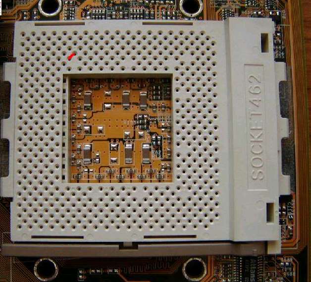
| 1. | If necessary unlock the Athlon XP Thoroughbred CPU using the wire trick, then reinstall the CPU and the heatsink (Athlon XP Barton is automatically unlocked to have access to the lower multiplier settings when mounted on the A7N8X in combination with the latest BIOS version). | |
|
The wire trick method to unlock Athlon XP Thoroughbred cpus. A fine copper wire is attached as a bridge in the marked holes as to get access to the lower multiplier settings. Source: AsusBoards Forums. |
|
| 2. | We will use an Athlon XP 2400+ to exemplify. It runs at 2000 MHz as default clock speed, so if you don't want to O/C, we’ll try to apply a multiplier setting to get as close as 2000 MHz. The formula used is: 2000 MHz (cpu clock speed) divided by 166 MHz (FSB setting) = 12. Now move to the BIOS and choose the "Menu" in the multiplier options and select 12x. | |
| 3. | There are some options for the CPU Interface. This sets the mode for CPU/FSB parameters usage. If you're only interested in 166MHz, you can choose the "Optimal" option. However, if you want to O/C you should select “Aggressive”. | |
| 4. | Proceed and adjust Memory Timing, which is one of the most important things to configure to achieve a stable system. Make sure that the memory work in sync with the FSB - set the Memory Frequency to “Sync”. | |
| 5. | Next you have to set the Memory Timings, where you select "User Defined". Most PC2700 are rated by default at 7-3-3-2.5 memory timings, if running at 166 MHz FSB, so you should insert the values in the “User Defined” menu. You can finally save, exit BIOS and re-boot. | |
![]()
Memory timing settings:
To tweak the memory settings you should go to BIOS and select “user defined” from the Memory Timing menu: In general, changes of the Sdram CAS latency will have the most dominant impact on speed and performance, the Sdram precharge delay will have less impact on speed but is of significant importance to stability, the Sdram RAS to CAS and Sdram RAS precharge delay values are of intermediate importance.
Some examples of default memory timing settings (in the following order: Sdram Active precharge-Sdram RAS to CAS delay-Sdram RAS precharge delay-Sdram CAS latency):
PC2100: 6-2-2-2T
PC2700: 7-3-3-2.5T
PC3200: 7-3-3-2T (Corsair PC3200LLPT)
PC3500: 5-2-2-2T (Corsair XMS PC3500)
When you intend to O/C the FSB it is crucial that you select memory with specs that can match the higher FSB settings and run in sync. To calculate what minimum memory speed you need with a tweaked FSB setting you proceed as follows: 8 bits/byte * 2 (double-clocked data with DDRRAM) * FSB speed.
![]()
Memory sync mode:
To get the nForce2 to run memory and FSB in 100% sync with each other, as to achieve best performance, you should configure the Memory Frequency menu to “Sync”. This should be considered as the default setting if you do not O/C the motherboard.
![]()
Memory configuration issues:
Crucial have verified that there are compatibility issues with their PC2700 512 Mb memory modules and the nForce2 chipset at 166 MHz (http://www.amdforums.com/). The verdict, based on users’ and techs’ reports, is to have PC3200 DDR RAM or higher of good quality in combination with the Asus A7N8X. It is also known that certain batches of Corsair XMS 3200 CAS2 and XMS 3500 CAS2 would cause the A7N8X to not post. The fix is to manually set the memory timings in BIOS to the following:
XMS3200 CAS 2:
DRAM Clock: 200 MHz
DRAM Timing (overrides SPD values): Manual
System Performance: Normal
Bank cycle time (or tRAS): 6
Bank Interleave: 4
RAS Precharge (tRP): 3
RAS-to-CAS Delay (tRCD): 3
CAS Latency: 2
Command Rate: 1T
Memory Voltage: motherboard default*
XMS3500 CAS 2:
CPU Speed: Manual
CPU External Frequency: 145
CPU to Memory FSB ratio: 4:6
SDRAM Configuration: Manual
SDRAM CAS Latency: 2T
SDRAM RAS to CAS Delay (tRCD): 3T
SDRAM RAS Precharge (tRP): 3T
SDRAM Active to Precharge Delay (tRAS): 7T
SDRAM Command Control: 1T
SDRAM Bank Interleave: 4 Banks
Memory Voltage: motherboard default*
You may be able to receive a-one-and-only boot opportunity after resetting the CMOS – the problem with these batches of Corsair modules is that without POST you cannot get into the BIOS menu. Newer Corsair modules do not have these problems as the programming of the memory has changed. There is currently no BIOS fix for this issue.
![]()
Athlon XP/333 MHZ FSB:
With the newer breed of Athlon XP Thoroughbred B/Barton3 CPUs it is possible to O/C the A7N8X to 185-195 MHz FSB4 settings with effective heatsink/cooling of the CPU but without additional active cooling of the Northbridge chipset. Compatible quality DDR RAM modules, robust PSUs with stable power at the separate voltage ramps and effective heatsink/cooling devices are prerequisites to succeed in O/C. TwinX PC3200 CAS2 memory modules (Corsair, Kingston) or higher are strongly recommended for anyone who aims to run the A7N8X at higher than default FSB settings. You will also need two memory modules to get dual channel memory performance positioned in either slot in 1 and 3 or in 2 and 3.
The new Athlon XP Barton cores are auto-unlocked in combination with the A7N8X motherboard (direct access to 5-12.5 multiplier settings in the BIOS menu).
From the tabulated data below it is concluded that the Athlon XP Barton CPUs are good performers in robust O/C without any major hardware modifications. As of this date the Athlon XP 2500+ Barton/ XP 2600+ 333 MHz FSB Thoroughbred show a comparatively favourable price:performance ratio (they also dissipate less heat per clock cycle than the older Athlon cores and the Barton is auto-unlocked with the A7N8X).
![]()
How to run the Athlon XP/333 Mhz stable at 200 MHz FSB:
It has recently been found that nForce2 motherboards prior to revision 2 for some reason destabilize when running Athlon XP/333 MHz and trying to O/C to 200 MHz FSB. Users have found that without modifications the old Athlon XP/266 O/C better than the Athlon XP/333.
On the A7N8X there are two alternative tricks/modifications to achieve improved stability with Athlon XP/333 MHz CPUs at FSB speeds over 190-195 MHz. The first modification, already schematically described in the former section, is based on moving the CPU_FSB jumper, placed on the motherboard, from the 266/333 position (pins 1 and 2) to the 200 position (pins 2 and 3). The following steps describe the procedure (discussed in more detail at Amdmb.com Forums):
| 1. | Shut down |
| 2. | Clear the CMOS |
| 3. | Move the CPU_FSB jumper from the 266/333 position to the 200 (from pins 1-2 to pins 2-3) |
| 4. | Reboot up, enter into BIOS, reset default values, apply any changes of your choice |
| 5. | Your memory now have to comply with the higher FSB speed and you should preferably add a heat sink to the Northbridge to deal with raised chipset temperature |
| 6. | You should be able to run at approx. 200 MHz FSB stable with decent air cooling |
The second trick, also applicable to nForce2 motherboards without the CPU_FSB jumper, includes the physical modification of one of the L12 bridges on the Athlon XP/333 CPU. Beware that this modification will void any warranty on the CPU! The one L12 bridge to be cut is illustrated in this picture:
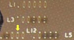
Location of the L12 bridge.
The yellow arrow indicates the location of the bridge to cut.
To cut the bridge you can preferably use a razor or X-acto knife. A magnifying glass may also be helpful. You don't need to cut very deeply as the wires are just below the substrate surface. You can test that you’ve cut sufficiently deep by using an ohm meter or by testing if the CPU boots (with default settings loaded) to a 133 MHz FSB, if so you're done—if not, cut a little deeper. This is a simple operation and actually won't take very long—but remember to be careful while you do it so not other bridges are being damaged.
![]()
3
refers to the Athlon XP Thoroughbred B 333 MHz FSB/Barton CPUs; for details
on model numbers and default clock speed go to Athlon
XP data;
4 actual and stable O/C performance will vary between single motherboards
| Nächste Seite | Vorherige Seite | |||||||
![]()
Copyright © 2002 RME. Alle Rechte vorbehalten.
RME ist ein eingetragenes Markenzeichen.
Diese Website enthält Namen und Marken anderer Firmen